Samsung to boost HBM5 speeds with cutting-edge 2-nanometer tech
The next-generation HBM5 memory will use a 2-nanometer base die to deliver faster performance, better power efficiency and stronger AI chip competitiveness.
A model of Samsung Electronics’ eighth-generation high bandwidth memory, HBM5, as seen at an exhibition in June.SAMSUNG ELECTRONICS
Samsung Electronics plans to apply its most advanced 2-nanometer process to HBM5, the next generation of high bandwidth memory (HBM), the company said Monday.
“HBM5 is expected to operate at speeds more than 50 percent faster than HBM4E,” Ku Ja-hum, executive vice president and head of technology development at Samsung Electronics' foundry business division, said in an interview posted on a corporate website.
“We plan to apply our most advanced process technology to a base die, which can significantly improve both operating speed and power efficiency.”
A base die refers to the bottom of an HBM stack, which serves as the interface that enables HBM to exchange data rapidly with the processor or accelerator.
Samsung will adopt its 2-nanometer process based on the gate-all-around (GAA) transistor architecture for the HBM5 base die while also implementing higher-density through-silicon via (TSV) technology, according to Ku.
TSV is a packaging technology that connects stacked dynamic random access memory (DRAM) chips by drilling microscopic holes through silicon and filling them with conductive electrodes. The memory chips are thinned to less than half the thickness of a sheet of paper.
Samsung Electronics highlighted its turnkey manufacturing capability as a key competitive advantage. It handles every stage of HBM production in-house, from design and fabrication to packaging.
Its HBM core die is manufactured at the memory business division, while the base die is produced by the foundry division. They are later packaged at its Test & System Package unit.
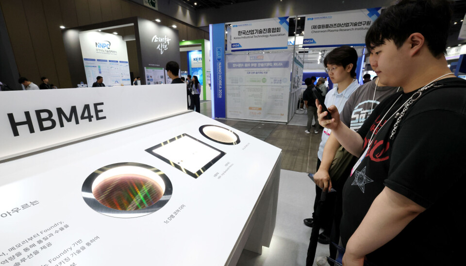
Visitors observe Samsung Electronics' high bandwidth memory product, HBM4E, at an exhibition in Gyeonggi on July 8.NEWS1
“As optimization is possible from the design stage, we can shorten the time needed to complete mass-production products while also improving cost competitiveness,” Ku said.
On the competitiveness of Samsung's Foundry business, the company began mass production of the world's first GAA-based 3-nanometer process and launched volume production of its first-generation 2-nanometer process in the second half of last year.
It also plans to begin mass production of mobile chips based on its second-generation 2-nanometer process, which offers improved yield and performance, in the second half of this year.
Samsung Electronics has received orders not only from mobile customers but also from major clients in AI, high-performance computing and cloud service providers, including EV maker Tesla.
“Our 4-nanometer process has also secured stable yields and competitive performance through years of mass-production experience,” Ku said. “We will continue expanding our share of the chip foundry market on the strength of our advanced process technologies.”
This article was originally written in Korean and translated by a bilingual reporter with the help of generative AI tools. It was then edited by a native English-speaking editor. All AI-assisted translations are reviewed and refined by our newsroom.